A contactless smart card (also known as a radio frequency card) is a new technology developed in recent years. It successfully implements the combination of Radio Frequency Identification (RFID) and smart card technology. The contactless smart card solves the problem of passive (no power in the card) and contactless, and is a breakthrough in the field of electronic devices. It not only has all the functions of contact smart card (including data processing function) and anti-counterfeit security, reliable reading and writing, simple reading and writing equipment, fast operation, etc., but also has many advantages that contact smart cards can't match. The RF interface of the contactless smart card that complies with the ISO/IEC 14443-2 standard has two standards: TYPE A and TYPE B. The TYPE A standard stipulates that the Proximity Coupling Device (PCD) is a Proximity Integrated Circuit Card (PICC) that uses a Miller-coded Amplitude Shift Keying signal with a modulation factor of 100%. Referred to as ASK), the PICC sends to the PCD an On-Off Keying (OOK) signal using Manchester encoding. The TYPE B standard stipulates that the PCD sends to the PICC a non-return-to-zero (NRZ) ASK signal with a modulation factor of 10%. The PICC transmits a subcarrier-modulated NRZ binary phase-shift keying signal (Binary Phase). Shift Keying (BPSK for short) is implemented with load modulation [1]. This paper mainly introduces the implementation of the modem module in the non-contact IC card that conforms to the TYPE B standard.
1 circuit design
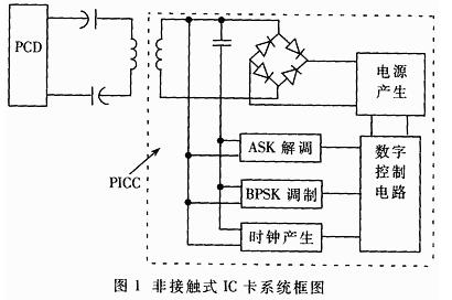
Figure 1 is a block diagram of a contactless IC card system. The PCD and PICC are coupled by a coil to implement half-duplex communication [1]. The PICC is a passive structure whose operating energy is obtained from the PCD by in-line coils through inductive coupling. The RF carrier signal is applied to the inductive coil of the PCD, causing a magnetic field to be generated around the PCD. When the PICC enters the magnetic field, energy is obtained by electromagnetic induction through a coil on the card. Data communication between each other can be achieved by changing the magnetic field strength between the PCD and the PICC.
1.1 BPSK modulation
The PICC transmits the BPSK signal of the NRZ, which is implemented by the load modulation method of the subcarrier. The clock generation circuit recovers the 13.56 MHz operating clock from the received signal, which is divided by 16 in the digital control circuit to produce a subcarrier signal of 847 kHz.
The modulation process is completed in two steps: first, the subcarrier signal is modulated by the digital signal to be transmitted to implement BPSK modulation; then the obtained binary PSK signal is superimposed on the carrier signal and transmitted [2].
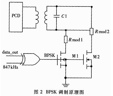
The schematic diagram of BPSK modulation is shown in Figure 2. The data_out to be transmitted and the subcarrier signal of 847 kHz are XORed to obtain the BPSK signal [3]. The BPSK signal controls the on and off of M1 and M2, and the carrier signal received by the PICC is modulated by the resistors Rmod1 and Rmod2 at a rate of 847 kHz. A modulation current is generated, represented by ΔI; the modulated signal affects the strength of the magnetic field generated by the PCD through the coupling action of the antenna, and the BPSK signal is sent to the PCD to implement load modulation. The value of the electromotive force (EMF) induced on the coil in the PCD is:
ΔV=2π·M·F·ΔI
Where M is the mutual inductance value and F is the carrier frequency.
1.2 ASK demodulation section
The PCD sends a 10% ASK signal at a rate of 106 kbps to ensure that the PICC can operate continuously. The data to be transmitted by the PCD is directly modulated on the RF carrier with a modulation factor of 10% (compared to the nominal amplitude, the "1" signal is 10% larger than the nominal amplitude. Correspondingly, the "0" signal is proportional to the nominal amplitude. 10% smaller). The demodulation portion of the PICC recovers digital information from the ASK signal [3].
The schematic diagram of the ASK demodulation part is shown in Figure 3. The circuit is mainly composed of an envelope detector "title="detector">detector, carrier filter and edge detector. The envelope detector can be composed of a PMOS bridge circuit. In order to prevent the power signal from interfering with it, an independent The bridge circuit is completed. Since many factors (such as distance, card direction, etc.) affect the amplitude value of the signal envelope, an edge detector is used to recover the NRZ data.
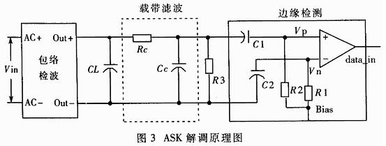
The carrier filter is a low-pass filter "title="low-pass filter">low-pass filter to filter the noise of the carrier ripple signal and is implemented with a RC first-order low-pass filter. Voltage Comparator" Title="Voltage Comparator">The two input terminals of the voltage comparator introduce the bias voltage through the resistors R1 and R2. On the other hand, the envelope signal detected by the envelope detector is also connected to the capacitor C1 after low-pass filtering. The non-inverting input of the voltage comparator. Obviously, when the circuit is stable, Vp=Vn=VBias, the output of the voltage comparator is 0; when receiving the 10% ASK signal, the voltage Vp of the non-inverting input of the voltage comparator will fluctuate with the change of AM. The inverting input is still VBias, so that the voltage comparator can detect the envelope change information of the ASK signal and demodulate the digital information.
2 simulation results
The design was simulated with the ADVANCED DESIGN SYSTEM software.
2.1 Simulation results of BPSK modulation circuit
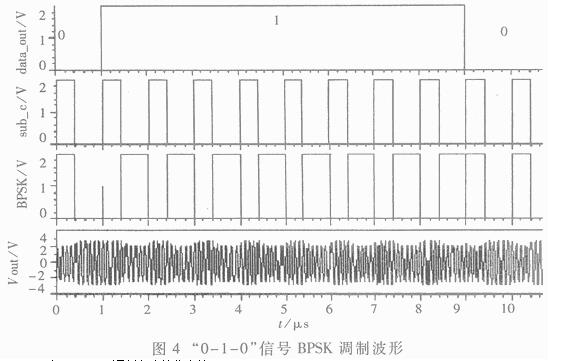
The transmitted data data_out rate is 106 kbps, and it is used to modulate the subcarrier signal sub_c of 847 kHz. When the transmitted data data_out is 0, the generated BPSK signal is in phase with sub_c; when data_out is 1, BPSK and sub_c are 180° out of phase. The BPSK signal controls the switches of M1 and M2 to realize load modulation, and the data_out signal is transmitted through the coupling action of the coil. That is, when the PICC transmits data, the signal frequency sensed by the PCD coil is still 13.56 MHz, and the amplitude changes with the change of the BPSK signal, as shown in FIG.
2.2 Simulation results of ASK demodulation circuit
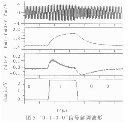
The PICC receives an ASK signal with a carrier frequency of 13.56 MHz and a modulation factor of 10% (shown as Vin in Figure 5), and the transmitted data rate is 106 kbps. After the envelope detection, the Vot signal is detected, and the signal is detected by the edge detector to recover the original data, as shown in FIG. 5.
This design can also be used in other ASK demodulation and BPSK modulation applications to achieve wireless data transmission and inter-device communication. The reliable card reading distance is 10cm. When the power supply voltage drops below 2V, the circuit can still work normally, and the total current consumption of the circuit is less than 5μA.
The module can be used as a stand-alone IP core. When fully integrated, it can reduce the number of system components and improve the stability of the system.
Bath Accessories Set,Bathroom Accessories,Bathroom Accessories Set,Luxury Bathroom Accessories
Jiangmen Chang Kun Industrial Co., Ltd. , https://www.changkun-houseware.com